- Contact Person : Mr. Wan Simon
- Company Name : Shenzhen Ciscoricky Technology Co., Ltd.
- Tel : 0086-755-29225636
- Fax : 0086-755-84886800
- Address : Guangdong,Shenzhen,Jinli Industry Park NO. 24 Mumian Road Buji Town
- Country/Region : China
- Zip : 518112
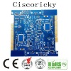
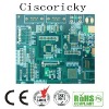
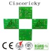
Rigid PCB Fabrication,pcb manufacturer ,pcb prototype
PCB types Gold plated PCB, tin plated PCB, immersion gold/silver/tin PCB, nickel-gold plated PCB, half-hole PCB, gold finger PCB, OSP board, carbon oil PCB, thick copper coil PCB, high TG PCB, Rogers HF PCB, high thermal conductivity aluminum PCB, blind and buried vias PCB, impedance control PCB and HDI PCB, as well as via holes, peelable adhesive, electrically conductive adhesive and all types and different colors of light-sensitive printing ink as required by customers.
Our PCB got UL,SGS,ISO9001,RoHS,QS9000 and TS16949 certificates,and are used to a wide range of fields such as computers,digital products,medical equipment,automobiles,communication devices, military,industrial control and aviation.
Key Specifications
Layer: 1 to 22 layers Materials: FR-4, CEM-3, Teflon, aluminum, Rogers, high Tg Surface finishing: lead-free HASL, immersion gold/tin/silver, OSP, gold finger plating, selective immersion gold and gold plating Maximum panel size: 550 x 650mm Minimum finished holes size: 0.10mm Finished holes tolerance: PTH: ±0.075mm NPTH: ±0.050mm Press fit: ±0.050mmAspect ratio: 9:1 Laser micro vias diameter: 0.10 to 0.15mm Aspect ratio: 1:1 Minimum line width/spacing: ½oz/18μm, 0.075/0.075mm 1oz/35μm, 0.15/0.15mm 2oz/70μm, 0.20/0.20mm 3oz/105μm, 0.25/0.25mmSolder mask: ±0.075mm Layer to layer: ±0.060mm Copper feature to holes (outer): ±0.075mm Minimum plated drills to copper (inner): 2 to 8L 0.25mm, 10 to 22L 0.30mm Edge to edge tolerance: ±0.100mm Holes to edge tolerance: ±0.100mm Minimum copper to edge distance: Outer: 0.25mm Inner: 0.40mmMaximum copper thickness: 140μm (4oz) Maximum board thickness: 4.80 mm Minimum board thickness: 2L 0.20mm, 4L 0.40mm, 6 to 22L 0.60mm Minimum core thickness: 0.10mm Minimum soldermask dam: 0.10mm Controlled impedance (Ω): ±7% to 10%PCB production capacity Double sided PCB :200000 ft2 /MonthMultilayer PCB :320000 ft2/MonthHDI PCB : 80000 ft2/Month
All of the above description is to demonstrate the ability of our PCB factory, if you have specific requirements, please feel free to contact us.
Rigid PCB Fabrication,pcb manufacturer ,pcb prototype


